Graduate School of Science and Engineering Electrical and Electronic Engineering
- Course Outline
- Opto-Electronics & Systems Laboratory
- Electrical and Electronic Materials Laboratory
- Laboratory for Electric Circuits and Systems
- Power System Analysis Laboratory
- High-frequency Engineering Laboratory
- Electrical Machinery & Apparatus Laboratory
- Laboratory of Ultrasonic Electronics
- Plasma Physics Laboratory
- Laboratory of Applied Mathematics
- Communication Systems Laboratory
- Laboratory for photonic devices
Laboratory for photonic devices
We aim to create environmentally friendly, low-cost, low-power consuming photonic devices with new functions to meet the needs of the near future.
Staff

OHTANI Naoki
[Professor]
| Acceptable course | |
|---|---|
| Master's degree course | ✓ |
| Doctoral degree course | ✓ |
Telephone : +81-774-65-6269
ohtani@mail.doshisha.ac.jp
Office : YE-119
Database of Researchers
Research Topics
- Optical properties of compound semiconductors and their application in laser and MEMS technology
- Improving organic EL device functions and elucidating device physics
- Realizing higher performance of organic thin-film solar cells
- Optical applications of anisotropic dielectric media
- Formation and application of functional fine structures
Research Contents
Many photonic devices are used around us. We often see them in lighting devices, displays of mobile phones and digital cameras, and solar cells, etc. With the start of fiber-optic Internet service for the consumer market, people now see that light is used in telecommunications. Telecommunications use lasers, photodetectors, modulators that place information in light, and amplifiers that boost light intensity.Photonic devices are already in widespread use, but demand for them is expected to continue growing with the advent of ubiquitous computing society. Accordingly, performance of photonic devices must improve, while the device must also become lower cost and smaller. To meet these needs, it is not sufficient to only boost the performance of the photonic devices already in use. We also need to develop new ideas that arise from investigations into the properties of new materials.
In light of this situation, the Laboratory for Photonic Devices seeks to "find materials and principles that will be useful in people's lives." To this end, we are studying the optical properties and fabrication technologies of new compound semiconductors and organic materials while exploring possibilities of high-performance photonic devices with new functions. We are divided into the four groups listed below, with one student in charge of each topic. Therefore, each student must learn everything needed for their topic, from ways to fabricate samples to evaluation methods. Students must also study programming technology for automating measuring instruments and calculation technology for theoretical evaluation of experimental data. These are technologies and knowledge that are sure to come in handy after students enter society.
Some of the keywords that appear often in these topics are "thin films," "quantum wells," the "nano" prefix and "quantum dots." These are collectively termed "nanotechnologies;" they attempt to apply new phenomena that occur in very small new substances, in the nanometer range, to new photonic devices.
1. Inorganic compound semiconductor group
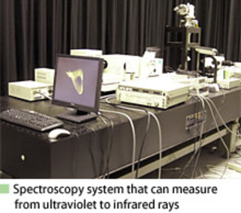
This group is evaluating the basic physical properties of antimony-nitrogen compound semiconductors, new materials that are so far little studied. We are studying these materials because they may make it possible to create photonic devices that can cover a broad range of wavelengths from deep ultraviolet to far infrared. Once their basic properties are elucidated, the group will try to fabricate multiple quantum wells and quantum dots from these new materials and fabricate light emitting diodes and optical modulators.
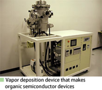
2. Organic low-molecular semiconductor group
Progress has been made in applying organic small molecules to displays, etc., but there is much that still remains unclear about the mechanisms of electron transport and emission properties in devices. One particular possibility is that we may be able to greatly improve emission properties and develop new emission mechanisms by creating nanostructures such as multiple quantum wells that combine different materials. We are also researching ways to fabricate nanowires, which will enable nanometer scale wiring that can make organic integrated circuits a reality.
3. Organic polymer semiconductor group
Organic polymers are effective for reducing the costs of devices because materials can be developed using simple manual procedures. In our group, we research ways to more simply achieve the emission properties of low-molecular materials by incorporating low-molecular materials into polymer materials. We are also developing new emission mechanisms that incorporate nanoparticles, fine metal particles, carbon nanotubes and the like to develop devices that emit ultraviolet and infrared rays.
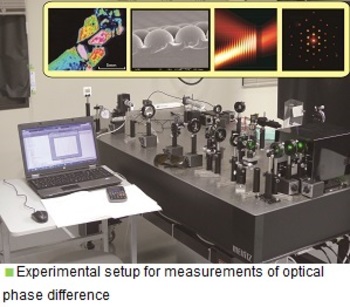
4. Applied Waveoptics Group
Our group develops functional optical devices and optical measuring techniques and explores applications of optical information processing using dielectric constant anisotropy media and microstructures. On the basis of optical physics, we study material properties, structures, and surfaces or interfaces to develop novel optical technologies.
Keywords
- Light-emitting device
- Photodetector
- Sensor device
- Quantum effect device
- Compound semiconductor
- Organic EL
- Organic thin-film solar cell
- Process technology
- Optical nonlinear material
- Nanostructure
- Quantum dot
- Colloidal particles
- Anisotropic dielectric media
- Form birefringence